 Q. No.
In the half-wave rectifier circuit shown. Which one of the following wave forms is true for , the output across C and D?


A full-wave rectifier circuit along with the input and output voltages is shown in the figure.

The contribution to the output voltage from diode – 2 is :
(1) A, C
(2) B, D
(3) B, C
(4) A, D
The i-V characteristic of a P-N junction diode is shown below. The approximate dynamic resistance of the P-N junction when a forward bias of 2 volt is applied

(1) 1
(2) 0.25
(3) 0.5
(4) 5


A 2V battery is connected across the points A and B as shown in the figure given below. Assuming that the resistance of each diode is zero in forward bias and infinity in reverse bias, the current supplied by the battery when its positive terminal is connected to A is

(a) 0.2 A
(b) 0.4 A
(c) Zero
(d) 0.1 A
In the circuit given below, V(t) is the sinusoidal voltage source, voltage drop (t) across the resistance R is

(a) Is half wave rectified
(b) Is full wave rectified
(c) Has the same peak value in the positive and negative half cycles
(d) Has different peak values during positive and negative half cycle
Ge and Si diodes conduct at 0.3 V and 0.7 V respectively. In the following figure if Ge diode connection are reversed, the valve of changes by

(1) 0.2 V
(2) 0.4 V
(3) 0.6 V
(4) 0.8 V


For the transistor circuit shown below, if = 100, voltage drop between emitter and base is 0.7 V, then value of will be :
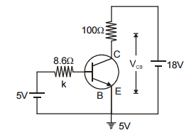
(1) 10 V
(2) 5 V
(3) 13 V
(4) 0 V


Figure gives a system of logic gates. From the study of truth table it can be found that to produce a high output (1) at R, we must have

(1) X = 0, Y = 1
(2) X = 1, Y = 1
(3) X = 1, Y = 0
(4) X = 0, Y = 0
© 2026 GoodEd Technologies Pvt. Ltd.