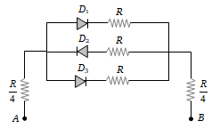
In the following circuits PN-junction diodes , and are ideal for the following potential of A and B, the correct increasing order of resistance between A and B will be

(i) – 10 V, – 5V (ii) – 5V, – 10 V
(iii) – 4V, – 12V
(a) (i) < (ii) < (iii) (b) (iii) < (ii) < (i)
(c) (ii) = (iii) < (i) (d) (i) = (iii) < (ii)

(iii) – 4V, – 12V
(c) (ii) = (iii) < (i) (d) (i) = (iii) < (ii)
The circuit shown in the following figure contains two diode and each with a forward resistance of 50 ohms and with infinite backward resistance. If the battery voltage is 6 V, the current through the 100 ohm resistance (in amperes) is
1. Zero
2. 0.02
3. 0.03
4. 0.036
The contribution in the total current flowing through a semiconductor due to electrons and holes are and respectively. If the drift velocity of electrons is times that of holes at this temperature, then the ratio of concentration of electrons and holes is
1. 6 : 5
2. 5 : 6
3. 3 : 2
4. 2 : 3
Ge and Si diodes conduct at 0.3 V and 0.7 V respectively. In the following figure if Ge diode connection are reversed, the valve of changes by
(1) 0.2 V
(2) 0.4 V
(3) 0.6 V
(4) 0.8 V
In the following circuit, find and .
(a) 0, 0
(b) 5 mA, 5 mA
(c) 5 mA, 0
(d) 0, 5 mA
For the transistor circuit shown below, if = 100, the voltage drop between emitter and base is 0.7 V, then the value of will be:

1. 10 V
2. 5 V
3. 13 V
4. 0 V
The following configuration of gate is equivalent to
1. NAND
2. XOR
3. OR
4. None of these
Figure gives a system of logic gates. From the study of truth table it can be found that to produce a high output (1) at R, we must have
(1) X = 0, Y = 1
(2) X = 1, Y = 1
(3) X = 1, Y = 0
(4) X = 0, Y = 0
The combination of gates shown below produces
(1) AND gate
(2) XOR gate
(3) NOR gate
(4) NAND gate
The figure shows two NAND gates followed by a NOR gate. Which of the following logic gate does the figure represent?

1. OR
2. AND
3. NAND
4. None of these


