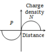
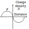
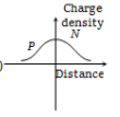
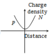
The curve between charge density and distance near P-N junction will be
1. 
2. 
3. 
4. 


The resistance of a germanium junction diode whose is shown in figure is
(1) 5 k
(2) 0.2 k
(3) 2.3 k
(4)
In the half-wave rectifier circuit shown. Which one of the following wave forms is true for , the output across C and D?

| 1. | 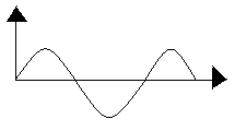 |
2. | 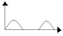 |
| 3. | 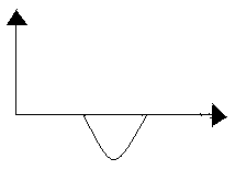 |
4. | 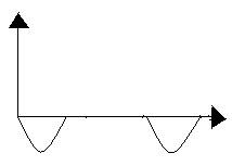 |
A full-wave rectifier circuit along with the input and output voltages is shown in the figure.
The contribution to the output voltage from diode – 2 is :
(1) A, C
(2) B, D
(3) B, C
(4) A, D
The i-V characteristic of a P-N junction diode is shown below. The approximate dynamic resistance of the P-N junction when a forward bias of 2 volt is applied
(1) 1
(2) 0.25
(3) 0.5
(4) 5
The given figure shows the wave forms for two inputs A and B and that for the output Y of a logic circuit. The logic circuit is
(1) An AND gate
(2) An OR gate
(3) A NAND gate
(4) An NOT gate
The variation of anode current in a triode corresponding to a change in grid potential at three different values of the plate potential is shown in the diagram. The mutual conductance of the triode is
1. 2.5 m mho
2. 5.0 m mho
3. 7.5 m mho
4. 10.0 m mho
A silicon specimen is made into a P-type semi-conductor by dopping, on an average, one Indium atom per silicon atoms. If the number density of atoms in the silicon specimen is then the number of acceptor atoms in silicon per cubic centimeter will be:
(1)
(2)
(3)
(4)
The probability of electrons to be found in the conduction band of an intrinsic semiconductor at a finite temperature
(1) Decreases exponentially with increasing band gap
(2) Increases exponentially with increasing band gap
(3) Decreases with increasing temperature
(4) Is independent of the temperature and the band gap
A 2V battery is connected across the points A and B as shown in the figure given below. Assuming that the resistance of each diode is zero in forward bias and infinity in reverse bias, the current supplied by the battery when its positive terminal is connected to A is
(a) 0.2 A
(b) 0.4 A
(c) Zero
(d) 0.1 A


