The temperature (T) dependence of resistivity (ρ) of a semiconductor is represented by

1. 

2. 

3. 

4. 

Subtopic:  Energy Band theory |
 73%
From NCERT
To view explanation, please take trial in the course.
NEET 2025 - Target Batch
Hints
To view explanation, please take trial in the course.
NEET 2025 - Target Batch

In a forward biased P-N junction diode, the potential barrier in the depletion region is of the form

1. 

2. 

3. 

4. 

Subtopic:  PN junction |
 56%
From NCERT
To view explanation, please take trial in the course.
NEET 2025 - Target Batch
Hints
To view explanation, please take trial in the course.
NEET 2025 - Target Batch

Different voltages are applied across a P-N junction and the currents are measured for each value. Which of the following graphs is obtained between voltage and current?

1. 

2. 

3. 

4. 

Subtopic:  PN junction |
From NCERT
To view explanation, please take trial in the course.
NEET 2025 - Target Batch
Hints
To view explanation, please take trial in the course.
NEET 2025 - Target Batch

advertisementadvertisement

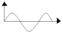
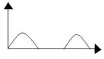
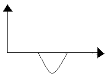
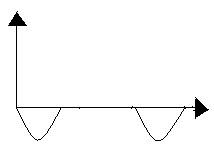
If the following input signal is sent through a PN-junction diode, then the output signal across RL will be


1. 

2. 

3. 

4. 

Subtopic:  PN junction |
 82%
From NCERT
To view explanation, please take trial in the course.
NEET 2025 - Target Batch
Hints
To view explanation, please take trial in the course.
NEET 2025 - Target Batch

The curve between charge density and distance near P-N junction will be

1. 
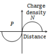
2. 
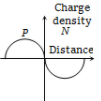
3. 
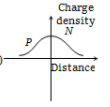
4. 
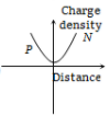
Subtopic:  PN junction |
From NCERT
To view explanation, please take trial in the course.
NEET 2025 - Target Batch
Hints
To view explanation, please take trial in the course.
NEET 2025 - Target Batch

The resistance of a germanium junction diode whose is shown in figure is Vk=0.3V


(1) 5 kΩ

(2) 0.2 kΩ

(3) 2.3 kΩ

(4) 102.3

Subtopic:  PN junction |
 71%
From NCERT
To view explanation, please take trial in the course.
NEET 2025 - Target Batch
Hints
To view explanation, please take trial in the course.
NEET 2025 - Target Batch

advertisementadvertisement

In the half-wave rectifier circuit shown. Which one of the following wave forms is true for VCD, the output across C and D?

1. 

2. 

3. 

4. 

Subtopic:  Rectifier |
 87%
From NCERT
To view explanation, please take trial in the course.
NEET 2025 - Target Batch
Hints
To view explanation, please take trial in the course.
NEET 2025 - Target Batch

A full-wave rectifier circuit along with the input and output voltages is shown in the figure.

The contribution to the output voltage from diode – 2 is :

(1) A, C                       

(2) B, D

(3) B, C                       

(4) A, D

Subtopic:  Rectifier |
 87%
From NCERT
To view explanation, please take trial in the course.
NEET 2025 - Target Batch
Hints
To view explanation, please take trial in the course.
NEET 2025 - Target Batch

The i-V characteristic of a P-N junction diode is shown below. The approximate dynamic resistance of the P-N junction when a forward bias of 2 volt is applied

(1) 1 Ω

(2) 0.25 Ω 

(3) 0.5 Ω

(4) 5 Ω

Subtopic:  PN junction |
 65%
From NCERT
To view explanation, please take trial in the course.
NEET 2025 - Target Batch
Hints
To view explanation, please take trial in the course.
NEET 2025 - Target Batch

advertisementadvertisement

The given figure shows the wave forms for two inputs A and B and that for the output Y of a logic circuit. The logic circuit is 

(1) An AND gate                   

(2) An OR gate

(3) A NAND gate                   

(4) An NOT gate

Subtopic:  Logic gates |
 86%
From NCERT
To view explanation, please take trial in the course.
NEET 2025 - Target Batch
Hints
To view explanation, please take trial in the course.
NEET 2025 - Target Batch