


The given circuit has two ideal diodes connected as shown in the figure below. The current flowing through the resistance \(R_1\) will be

1. \( 2.5\text{ A}\)
2. \( 10\text{ A}\)
3. \(1.43\text{ A}\)
4. \(3.13\text{ A}\)


The given graph represents the \(V\text-I\) characteristics of a semiconductor device. Which of the following statements is correct?

| 1. | It is a \(V\text-I\) characteristic of a solar cell where the point \(A\) represents open-circuit voltage and the point \(B\) represents short-circuit current. |
| 2. | It is for a solar cell and points \(A\) and \(B\) represents open-circuit voltage and current respectively. |
| 3. | It is for a photodiode and points \(A\) and \(B\) represents open-circuit voltage and current respectively. |
| 4. | It is for an LED and points \(A\) and \(B\) represents open-circuit voltage and short-circuit current respectively. |


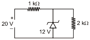
A Zener diode, having breakdown voltage equal to \(15\) V, is used in a voltage regulator circuit, as shown in the figure. The current through the diode is:
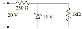
1. \(10\) mA
2. \(15\) mA
3. \(20\) mA
4. \(5\) mA
A p-n photodiode is fabricated from a semiconductor with a band gap of It can detect a signal of wavelength
1.
2.
3.
4.
A p-n photodiode is made of a material with a band gap of 2.0 eV. The minimum frequency of the radiation that can be absorbed by the material is nearly
1.
2.
3.
4.


PN-junction diode works as a insulator, if connected
(1) To A.C.
(2) In forward bias
(3) In reverse bias
(4) None of these
The PN junction diode is used as
(1) An amplifier
(2) A rectifier
(3) An oscillator
(4) A modulator
Zener breakdown in a semi-conductor diode occurs when
(1) Forward current exceeds certain value
(2) Reverse bias exceeds certain value
(3) Forward bias exceeds certain value
(4) Potential barrier is reduced to zero


When the P end of P-N junction is connected to the negative terminal of the battery and the N end to the positive terminal of the battery, then the P-N junction behaves like
(1) A conductor
(2) An insulator
(3) A super-conductor
(4) A semi-conductor
© 2026 GoodEd Technologies Pvt. Ltd.