
 Q. No.
Following diagram performs the logic function of:
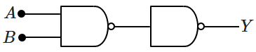
1. AND gate
2. NAND gate
3. OR gate
4. XOR gate
1. AND gate
2. NAND gate
3. OR gate
4. XOR gate


The barrier potential of a \(\mathrm{p\text-n}\) junction diode does not depend on:
| 1. | diode design | 2. | temperature |
| 3. | forward bias | 4. | doping density |
If a full-wave rectifier circuit is operating from \(50~\text{Hz}\) mains, the fundamental frequency in the ripple will be:
1. \(25~\text{Hz}\)
2. \(50~\text{Hz}\)
3. \(70.7~\text{Hz}\)
4. \(100~\text{Hz}\)


Reverse bias applied to a junction diode:
| 1. | lowers the potential barrier |
| 2. | raises the potential barrier |
| 3. | increases the majority carrier current |
| 4. | increases the minority carrier's current |
The current \((I)\) in the circuit will be:

| 1. | \(\dfrac{5}{40}~\text{A}\) | 2. | \(\dfrac{5}{50}~\text{A}\) |
| 3. | \(\dfrac{5}{10}~\text{A} \) | 4. | \(\dfrac{5}{20}~\text{A}\) |
The following truth table represent which logic gate:
| A | B | C |
| 1 | 1 | 0 |
| 0 | 1 | 1 |
| 1 | 0 | 1 |
| 0 | 0 | 1 |
1. XOR
2. NOT
3. NAND
4. AND


For the given circuit of the \(\mathrm{p\text-n}\) junction diode, which of the following statements is correct?

| 1. | In F.B. the voltage across \(R\) is \(V.\) |
| 2. | In R.B. the voltage across \(R\) is \(V.\) |
| 3. | In F.B. the voltage across \(R\) is \(2V.\) |
| 4. | In R.B. the voltage across \(R\) is \(2V.\) |
| A | B | Y |
| \(1\) | \(1\) | \(0\) |
| \(0\) | \(1\) | \(1\) |
| \(1\) | \(0\) | \(1\) |
| \(0\) | \(0\) | \(1\) |
2. XOR
3. NOR
4. OR

| 1. | High potential at the \(\mathrm{n}\) side and low potential at the \(\mathrm{p}\) side. |
| 2. | High potential at the \(\mathrm{p}\) side and low potential at the \(\mathrm{n}\) side. |
| 3. | \(\mathrm{p}\) and \(\mathrm{n}\) both are at the same potential. |
| 4. | Undetermined. |


The output of the OR gate is \(1\):
| 1. | if either or both inputs are \(1.\) |
| 2. | only if both inputs are \(1.\) |
| 3. | if either input is zero |
| 4. | if both inputs are zero |
© 2025 GoodEd Technologies Pvt. Ltd.