
 Q. No.
Identify the incorrect statement from the following:
1.
The resistivity of a semiconductor increases with an increase in temperature.
2.
Substances with an energy gap of the order of 10 eV are insulators.
3.
In conductors, the valence and conduction bands may overlap.
4.
The conductivity of a semiconductor increases with an increase in temperature.


Application of a forward bias to a p-n junction:
| 1. | widens the depletion zone. |
| 2. | increases the number of donors on the n side. |
| 3. | increases the potential difference across the depletion zone. |
| 4. | increases the electric field in the depletion zone. |
Of the diodes shown in the following diagrams, which one of the diodes is reverse biased?
| 1. |  |
2. | 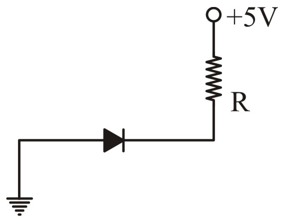 |
| 3. | 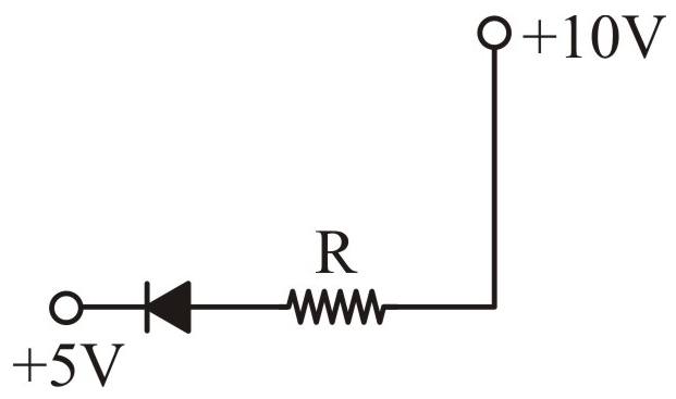 |
4. | 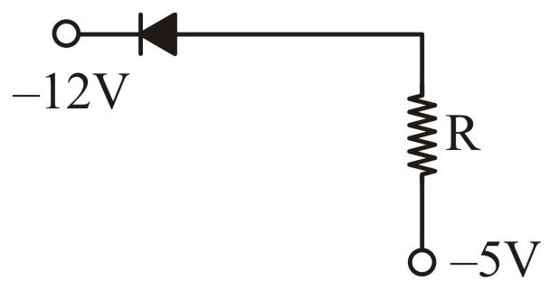 |


In semiconductors at room temperature:
| 1. | The valence band is completely filled and the conduction band is partially filled. |
| 2. | The valence band is completely filled. |
| 3. | The conduction band is completely empty. |
| 4. | The valence band is partially empty and the conduction band is partially filled. |
The peak voltage in the output of a half-wave diode rectifier fed with a sinusoidal signal without a filter is \(10\) V. The d. c. component of the output voltage is:
1. \(\frac{10}{\pi }\) V
2. \(10\) V
3. \(\frac{20}{\pi }\) V
4. \(\frac{10}{\sqrt{2}}\) V
For the given circuit of the P-N junction diode, which of the following statements is correct?
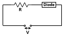
| 1. | In F.B. the voltage across R is V. |
| 2. | In R.B. the voltage across R is V. |
| 3. | In F.B. the voltage across R is 2V. |
| 4. | In R.B. the voltage across R is 2V. |
Reverse-bias applied to a junction diode:
| 1. | lowers the potential barrier |
| 2. | raises the potential barrier |
| 3. | increases the majority carrier current |
| 4. | increases the minority carrier's current |
The barrier potential of a p-n junction diode does not depend on:
1. diode design
2. temperature
3. forward bias
4. doping density
The V-I characteristic of a silicon diode is shown in the figure. The resistance of the diode at is:

Hole is:
| 1. | an anti-particle of electron. |
| 2. | a vacancy created when an electron leaves a covalent bond. |
| 3. | absence of free electrons. |
| 4. | an artificially created particle. |
© 2024 GoodEd Technologies Pvt. Ltd.