
 Q. No.
In the energy band diagram of a material shown below, the open circles and filled circles denote holes and electrons respectively. The material is a/an:

1.
p-type semiconductor
2.
insulator
3.
metal
4.
n-type semiconductor


The given circuit has two ideal diodes connected as shown in the figure below. The current flowing through the resistance R1 will be:

| 1. | 2.5 A | 2. | 10.0 A |
| 3. | 1.43 A | 4. | 3.13 A |
A forward-biased diode is treated as:
| 1. | an open switch with infinite resistance. |
| 2. | a closed switch with a voltage drop of 0 V. |
| 3. | a closed switch in series with a battery with voltage of 0.7 V. |
| 4. | a closed switch in series with small resistance and a battery. |


A half-wave rectifier voltage is fed to a load resistor. For which part of the cycle, the load current will flow?
| 1. | \(0^\circ-90^\circ\) | 2. | \(90^\circ-180^\circ\) |
| 3. | \(0^\circ-180^\circ\) | 4. | \(0^\circ-360^\circ\) |
In the given circuit, PN-junction diodes are ideal. For the following potential of A and B, the correct increasing order of resistance between A and B will be:

i. –10V, –5V
ii. –5V, –10V
iii. –4V, –12V
1. (i) < (ii) < (iii)
2. (iii) < (ii) < (i)
3. (ii) = (iii) < (i)
4. (i) = (iii) < (ii)
The depletion layer in the P–N junction region is caused by:
| 1. | the drift of holes |
| 2. | diffusion of charge carriers |
| 3. | migration of impurity ions |
| 4. | drift of electrons |
Carbon, silicon, and germanium have four valence electrons each. These are characterized by valence and conduction bands separated by the energy bandgap respectively equal to \((E_g)_C, (E_g)_{Si}~\text{and}~(E_g)_{Ge}\). Which of the following statements is true?
| 1. | \((E_g)_{Si} < (E_g)_{Ge}<(E_g)_{C}\) |
| 2. | \((E_g)_{C} < (E_g)_{Ge}>(E_g)_{Si}\) |
| 3. | \((E_g)_{C} > (E_g)_{Si}>(E_g)_{Ge}\) |
| 4. | \((E_g)_{C} =(E_g)_{Si}=(E_g)_{Ge}\) |
In the circuit shown, are respectively:
(If diodes are ideal)

1. 0, 0
2. 5 mA, 5 mA
3. 5 mA, 0
4. 0, 5 mA
The \((I-V)\) characteristics of a \(p-n\) junction diode is as shown. If \(R_1\) and \(R_2\) be the dynamic resistance of the \(p-n\) junction when (i) a forward bias of \(1\) volt is applied and (ii) a forward bias of \(2\) volts is applied respectively, then \(\frac{R_1}{R_2}=?\)

1. \(160\)
2. \(16\)
3. \(1.6\)
4. \(0.16\)
What is the equivalent resistance across the terminals of the battery if the diodes are ideal?
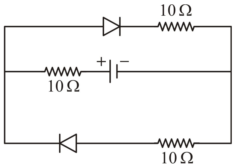
| 1. | \(10~ \Omega\) | 2. | \(20~ \Omega\) |
| 3. | \(15~ \Omega\) | 4. | \({10\over3} ~ \Omega\) |
© 2024 GoodEd Technologies Pvt. Ltd.