
 Q. No.
If in a \(\mathrm{p\text{-}n}\) junction, a square input signal of \(10~\text{V}\) is applied as shown,

then the output across \(R_L\) will be:
1.

2.

3.

4.

then the output across \(R_L\) will be:


Which logic gate is represented by the following combination of logic gates?

2. \(\mathrm{NAND}\)
3. \(\mathrm{AND}\)
4. \(\mathrm{NOR}\)
The given graph represents the \(\mathrm{V\text{-} I}\) characteristic for a semiconductor device.
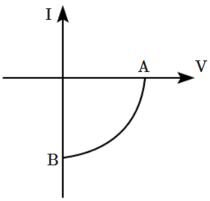
Which of the following statement is correct?
| 1. | It is a \(\mathrm{V\text{-} I}\) characteristic for the solar cell where point \(\mathrm{A}\) represents open-circuit voltage and point \(\mathrm{B}\) short circuit current. |
| 2. | It is for a solar cell and points \(\mathrm{A}\) and \(\mathrm{B}\) represent open-circuit voltage and current, respectively. |
| 3. | It is for a photodiode and points \(\mathrm{A}\) and \(\mathrm{B}\) represent open-circuit voltage and current respectively. |
| 4. | It is for a LED and points \(\mathrm{A}\) and \(\mathrm{B}\) represent open circuit voltage and short circuit current, respectively. |


The barrier potential of a \(\mathrm{p\text{-}n}\) junction depends on:
| (a) | type of semiconductor material |
| (b) | amount of doping |
| (c) | temperature |
Which one of the following is correct?
1. (a) and (b) only
2. (b) only
3. (b) and (c) only
4. (a), (b) and (c)
| 1. | Electrons are minority carriers and pentavalent atoms are dopants. |
| 2. | Holes are minority carriers and pentavalent atoms are dopants. |
| 3. | Holes are the majority carriers and trivalent atoms are dopants. |
| 4. | Electrons are the majority carriers and trivalent atoms are dopants. |
The output \((X)\) of the logic circuit shown in the figure will be:
1. \(X= \overline{A\cdot B}\)
2. \(X = A\cdot B\)
3. \(X= \overline{A+ B}\)
4. None of the above


Two ideal diodes are connected to a battery as shown in the circuit. The current supplied by the battery is:

| 1. | \(0.75~\text{A}\) | 2. | zero |
| 3. | \(0.25~\text{A}\) | 4. | \(0.5~\text{A}\) |
| 1. | in the case of \(\mathrm{C},\) the valence band is not completely filled at absolute zero temperature. |
| 2. | in the case of \(\mathrm{C},\) the conduction band is partly filled even at absolute zero temperature. |
| 3. | the four bonding electrons in the case of \(\mathrm{C}\) lie in the second orbit, whereas in the case of \(\mathrm{Si},\) they lie in the third. |
| 4. | the four bonding electrons in the case of \(\mathrm{C}\) lie in the third orbit, whereas for \(\mathrm{Si},\) they lie in the fourth orbit. |
The figure shows a logic circuit with two inputs \(A\) and \(B\) and the output \(C\). The voltage waveforms across \(A\), \(B\), and \(C\) are as given. The logic circuit gate is:

1. \(\text{OR}\) gate
2. \(\text{NOR}\) gate
3. \(\text{AND}\) gate
4. \(\text{NAND}\) gate


The symbolic representation of four gates is shown as:
Pick out which ones are for AND, NAND, and NOT gates, respectively.

1. (i), (iv), and (iii)
2. (ii), (iii), and (iv)
3. (ii), (iv), and (iii)
4. (ii), (iv), and (i)
© 2025 GoodEd Technologies Pvt. Ltd.