
 Q. No.
In the given figure, the potential difference between \(A\) and \(B\) is:

1.
\(0\)
2.
\(5\) volt
3.
\(10\) volt
4.
\(15\) volt


In a common-emitter transistor amplifier, the audio signal voltage across the collector is 3 V. The resistance of the collector is 3 k. If the current gain is 100 and the base resistance is 2 k, the voltage and power gain of the amplifier are:
1. 200 and 1000
2. 15 and 200
3. 150 and 15000
4. 20 and 2000
If in a \(\mathrm{p\text-n}\) junction, a square input signal of \(10\) V is applied as shown, then the output across \(R_L\) will be:

| 1. |  |
2. |  |
| 3. |  |
4. |  |


The given graph represents the \(V\text-I\) characteristic for a semiconductor device. Which of the following statement is correct?

| 1. | It is a \(V\text-I\) characteristic for a solar cell where point \(A\) represents open-circuit voltage and point \(B\) represents short-circuit current. |
| 2. | It is for a solar cell and points \(A\) and \(B\) represent open-circuit voltage and current respectively. |
| 3. | It is for a photodiode and points \(A\) and \(B\) represent open-circuit voltage and current respectively. |
| 4. | It is for a LED and points \(A\) and \(B\) represent open-circuit voltage and short circuit current respectively. |
Transfer characteristic [output voltage vs input voltage ] for a base biased transistor in CE configuration is as shown in the figure. For using transistor as a switch, it is used:

1. in region III
2. both in region (I) and (III)
3. in region II
4. in region I
| 1. | \(\mathrm{n}\text-\)type with electron concentration \(n_{e}=5\times10^{22}~\text{m}^{-3}\) |
| 2. | \(\mathrm{p}\text-\)type with electron concentration \(n_{e}=2.5\times10^{23}~\text{m}^{-3}\) |
| 3. | \(\mathrm{n}\text-\)type with electron concentration \(n_{e}=2.5\times10^{10}~\text{m}^{-3}\) |
| 4. | \(\mathrm{p}\text-\)type with electron concentration \(n_{e}=5\times10^{9}~\text{m}^{-3}\) |
A Zener diode, having breakdown voltage equal to \(15\) V, is used in a voltage regulator circuit, as shown in the figure. The current through the diode is:
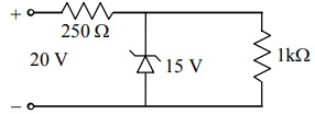
1. \(10\) mA
2. \(15\) mA
3. \(20\) mA
4. \(5\) mA
For transistor action:
| (a) | the base, emitter and collector regions should have similar size and doping concentrations. |
| (b) | the base regions must be very thin and lightly doped. |
| (c) | the emitter-base junction is forward biased and the base-collector junction is reverse biased. |
| (d) | both the emitter-base junction as well as the base-collector junction are forward biased. |
Which of the following pairs of statements is correct?
1. (d) and (a)
2. (a) and (b)
3. (b) and (c)
4. (c) and (d)
Carbon, Silicon, and Germanium atoms have four valence electrons each. Their valence and conduction bands are separated by energy gaps represented by \(\left(E_g\right)_C,(E_g)_{Si}~\text{and}~(E_g)_{Ge}\) respectively. Which one of the following relationships is true in their case?
| 1. | \(\left(E_g\right)_C<\left(E_g\right)_{G e} \) | 2. | \(\left(E_g\right)_C>\left(E_g\right)_{S i} \) |
| 3. | \(\left(E_g\right)_C=\left(E_g\right)_{S i} \) | 4. | \(\left(E_g\right)_C<\left(E_g\right)_{S i}\) |
| 1. | the current in the reverse biased condition is generally very small. |
| 2. | the current in the reverse biased condition is small but the forward-biased current is independent of the bias voltage. |
| 3. | the reverse-biased current is strongly dependent on the applied bias voltage. |
| 4. | the forward-biased current is very small in comparison to reverse-biased current. |
© 2024 GoodEd Technologies Pvt. Ltd.