
 Q. No.
The input resistance of a silicon transistor is 100 Ω. If the base current is changed by 40 µA, it results in a change in collector current by 2 mA. This transistor is used as a common emitter amplifier with a load resistance of 4 kΩ. The voltage gain of the amplifier is:
1. 3000
2. 4000
3. 1000
4. 2000


The following figure shows a logic gate circuit with two inputs \(A\) and \(B\), and the output \(Y\). The voltage waveforms of \(A,B\) and \(Y\) are as given.

The logic gate is:
| 1. | OR gate | 2. | AND gate |
| 3. | NAND gate | 4. | NOR gate |
The following table is for which logic gate?
| Input | Output | |
| A | B | C |
| 0 | 0 | 1 |
| 0 | 1 | 1 |
| 1 | 0 | 1 |
| 1 | 1 | 0 |
1. AND
2. OR
3. NAND
4. NOT


Zener diode is used for:
1. rectification.
2. stabilisation.
3. amplification.
4. producing oscillations in an oscillator.
| \(A\) | \(B\) | \(Y\) |
| \(1\) | \(1\) | \(1\) |
| \(1\) | \(0\) | \(0\) |
| \(0\) | \(1\) | \(0\) |
| \(0\) | \(0\) | \(0\) |
2. AND
3. NOR
4. OR
| 1. | The resistivity of a semiconductor increases with an increase in temperature. |
| 2. | Substances with an energy gap of the order of \(10\) eV are insulators. |
| 3. | In conductors, the valence and conduction bands may overlap. |
| 4. | The conductivity of a semiconductor increases with an increase in temperature. |
| 1. | widens the depletion zone. |
| 2. | increases the number of donors on the n side. |
| 3. | increases the potential difference across the depletion zone. |
| 4. | increases the electric field in the depletion zone. |
If a common emitter circuit is used as an amplifier, its current gain is \(50.\) If input resistance is \(1\) kΩ and input voltage is \(5\) V, then output current will be:
1. \(250\) mA
2. \(30\) mA
3. \(50\) mA
4. \(100\) mA
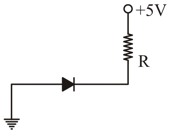
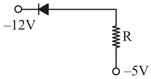
Of the diodes shown in the following diagrams, which one of the diodes is reverse biased?
| 1. |  |
2. |  |
| 3. | 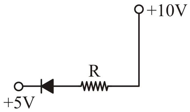 |
4. |  |
The truth table for the following network is:

| 1. |
|
|||||||||||||||
| 2. |
|
|||||||||||||||
| 3. |
|
|||||||||||||||
| 4. | None of the above |
© 2024 GoodEd Technologies Pvt. Ltd.