
 Q. No.
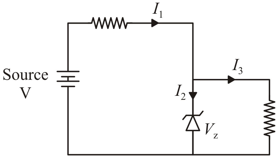
A Zener diode is shown in the following circuit diagram. When the source voltage fluctuates such that \(V>V_z\) then:
1.
all the current \(I_1, I_2~\text{and}~I_3\) change.
2.
only \(I_1\) and \(I_2\) change and \(I_3\) remains constant.
3.
only \(I_1\) and \(I_3\) change and \(I_2\) remains constant.
4.
all the currents remain constant.


When the emitter current increases by 10 mA, the base current increases by 0.4 mA. The value of voltage gain in the common emitter configuration of the amplifier will be:
(output and input resistance ratio is 50)
1. 1200
2. 1250
3. 150
4. 120


The net charges on -type semiconductor and -type semiconductor are, respectively:
| 1. | Positive, negative | 2. | Negative, positive |
| 3. | Positive, positive | 4. | Zero, zero |
| 1. | Forward biasing | 2. | Reverse biasing |
| 3. | No biasing | 4. | All of these |
1. \(2\) A and zero
2. \(3\) A and \(2\) A
3. \(2\) A and \(3\) A
4. zero and \(2\) A
If in a reverse-biased \(\mathrm{p\text-n}\) junction, an increase in carrier concentration takes place due to the creation of new hole-electron pairs by the light of wavelength less than or equal to \(620\) nm, then the bandgap is:
1. \(1\) eV
2. \(2\) eV
3. \(20\) eV
4. \(0.2\) eV
| 1. |  |
2. |  |
| 3. |  |
4. |  |
A n-p-n transistor operates in a common emitter mode as shown. The value of \(R_{L}\) is:
\(\small\left ( \text{Given,}I_{C}=4 mA,~V_{CE}=4~V,V_{BE}=0.6~V~\text{and}~\beta _{dc}=100 \right )\\\)

1. 1 k
2. 2 k
3. 3 k
4. 4 k
| 1. | It requires a low operational voltage. |
| 2. | It has a fast on-off switching capability. |
| 3. | The bandwidth of the emitted light is \(100\) A to \(10000\) A. |
| 4. | It does not require warm-up time. |
© 2024 GoodEd Technologies Pvt. Ltd.