
 Q. No.
In the following figure, the diodes which are forward biased are:
(a)

(b)

(c)

(d)

1. (a), (b) and (d)
2. (c) only
3. (a) and (c)
4. (b) and (d)
2. (c) only
3. (a) and (c)
4. (b) and (d)


| 1. | \(p\)-type with electron concentration \(n_e=5\times10^9~\text{m}^{-3}\). |
| 2. | \(n\)-type with electron concentration \(n_e=5\times10^{22}~\text{m}^{-3}\). |
| 3. | \(p\)-type with electron concentration \(n_e=2.5\times10^{10}~\text{m}^{-3}\). |
| 4. | \(n\)-type with electron concentration \(n_e=2.5\times10^{23}~\text{m}^{-3}\). |
The following figure shows a logic gate circuit with two inputs \(A\) and \(B\), and the output \(Y\). The voltage waveforms of \(A,B\) and \(Y\) are as given.

The logic gate is:
| 1. | OR gate | 2. | AND gate |
| 3. | NAND gate | 4. | NOR gate |


A Zener diode, having a breakdown voltage equal to 15 V, is used in a voltage regulator circuit as shown in the figure. The current through the diode is:
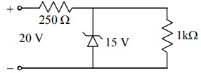
1. 5 mA
2. 10 mA
3. 15 mA
4. 20 mA
To get output \(Y = 1\) in the given circuit which of the following input will be correct?

| \(A\) | \(B\) | \(C\) | |
| 1. | 1 | 0 | 1 |
| 2. | 1 | 1 | 0 |
| 3. | 0 | 1 | 0 |
| 4. | 1 | 0 | 0 |

1. \(\mathrm{AND}\) gate
2. \(\mathrm{NOR}\) gate
3. \(\mathrm{OR}\) gate
4. \(\mathrm{NOT}\) gate
| 1. | the attraction of free electrons of the \(\mathrm{n\text{-}}\)region. |
| 2. | the higher hole concentration in the \(\mathrm{p\text{-}}\)region than that in the \(\mathrm{n\text{-}}\)region. |
| 3. | the higher concentration of electrons is in the \(\mathrm{p\text{-}}\)region than that in the \(\mathrm{n\text{-}}\)region. |
| 4. | the potential difference across the \(\mathrm{p\text{-}n}\) junction. |
The following figure shows a logic gate circuit with two inputs A and B and the output C. The voltage waveforms of A, B, and C are as shown below:
The logic circuit gate is:

1. AND gate
2. NAND gate
3. NOR gate
4. OR gate


In the energy band diagram of a material shown below, the open circles and filled circles denote holes and electrons respectively. The material is a/an:
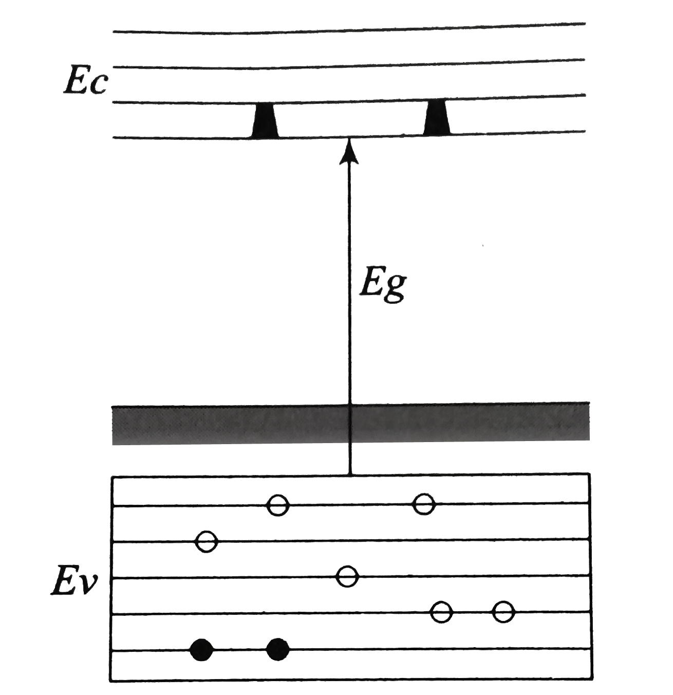
1. p-type semiconductor
2. insulator
3. metal
4. n-type semiconductor
© 2024 GoodEd Technologies Pvt. Ltd.