The forbidden gap in the energy bands of germanium at room temperature is about
1. 1.1 eV
2. 0.1 eV
3. 0.67 eV
4. 6.7 eV
Zener diode is used for
1. Rectification
2. Amplification
3. Stabilization
4. Modulation
For a common emitter configuration, if have their usual meaning, the incorrect relationship between is:
1.
2.
3.
4.
A semiconductor is known to have an electron concentration of and hole concentration . The semiconductor is
1. n type
2. p type
3. Intrinsic
4. None of these
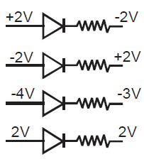
The forward-biased diode is
1. A
2. B
3. C
4. D
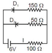
The circuit shown in the figure contains two diodes each with a forward resistance of 50 ohms and with infinite backward resistance. If the battery voltage is 6 V, the current through the 100-ohm resistance (in Amperes) is
1. Zero
2. 0.02
3. 0.03
4. 0.036
The electrical resistance of the depletion layer is large because:
| 1. | It has no charge carriers. |
| 2. | A potential difference is applied across carriers. |
| 3. | It contains electrons as charge carriers. |
| 4. | It has holes as charge carriers. |
The electrical conductivity of a semiconductor increases when electromagnetic radiation of a wavelength shorter than 2480 nm is incident on it. Find the bandgap of the semiconductor. Given Js,
1.
2.
3.
4.
The following truth table belongs to which one of the following four gate?
A B Y
1 1 0
1 0 0
0 1 0
0 0 1
1. OR
2. NAND
3. XOR
4. NOR
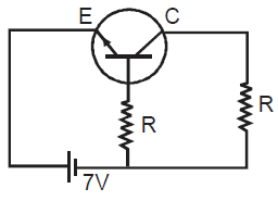
In the given transistor circuit, the base current is the value of is
1. 100
2. 200
3. 300
4. 400
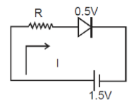
The diode used in the circuit shown in the figure has a constant voltage drop of 0.5 V at all currents and a maximum power rating of 100 milli-watts. What should be the value of the resistor R, connected in series with the diode, for obtaining maximum current?
1. 1.5
2. 5
3. 6.67
4. 200
Following diagram performs the logic function of
1. OR gate
2. XOR gate
3. AND gate
4. NAND gate
The number densities of electron and holes in pure silicon at are equal and its value is . On dropping with indium, the hole density increase to . What is the type of semiconductor? What is the electron density in doped silicon?
1.
2.
3.
4.
A Ge specimen is doped with Al. The concentration of acceptor atoms is . Given that the intrinsic concentration of electrons in the specimen is . The new electron concentration is
1.
2.
3.
4.
For a transistor, the current amplification factor is 0.8. The transistor is connected in a common emitter configuration. The change in the collector current when the base current changes by 6 mA is-
1. 6 mA
2. 4.8 mA
3. 24 mA
4. 8 mA
The transfer ratio of a transistor is 50. The input resistance of the transistor, when used in common emitter configuration, is . The peak value of the collector AC current for an AC input voltage of 0.01 V peak is
1. 100
2. 250
3. 500
4. 800
What is the voltage gain in a common emitter amplifier, where input resistance is 3 and load resistance 24? Take = 0.6
1. 8.4
2. 4.8
3. 2.4
4. 1.2
An n-type of semiconductor is formed by adding impurity materials
1. Aluminium, boron or selenium.
2. Aluminium, boron or indium.
3. Phosphorus, antimony or arsenic.
4. Cobalt, aluminium or selenium.
In a good conductor, the energy gap between the conduction band and the valence band is
1. Infinity
2. Wide
3. Narrow
4. Zero