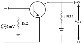
In the following common emitter configuration an npn transistor with current gain = 100 is used. The output voltage of the amplifier will be:
1. 10mV
2. 0.1 V
3. 1.0 V
4. 10 V
A Ge specimen is doped with Al. The concentration of acceptor atoms is ~ atoms/ . Given that the intrinsic concentration of electron-hole pairs is ~/, the concentration of electrons in the specimen is-
1.
2.
3.
4.
Which logic gate is represented by the following combination of logic gates ?
1. OR
2. NAND
3. AND
4. NOR
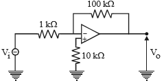
The voltage gain of the following amplifier is
1. 10
2. 100
3. 1000
4. 99
Which of the following logic gates is an universal gate ?
1. OR
2. NOT
3. AND
4. NAND
Consider an n-p-n transistor amplifier in common emitter configuration. The current gain of the transistor is 100. If the collector current changes by 1mA, what will be the change in emitter current
1. 1.1 mA
2. 1.01 mA
3. 0.01 mA
4. 10 mA
A transistor is a/an
1. chip
2. insulator
3. semiconductor
4. metal
If collector current is 120 mA and base current is 2 mA and resistance gain is 3, what is power gain?
1. 180
2. 10800
3. 1.8
4. 18
If in a p-n junction diode, a square input signal of 10 V is applied as shown
Then the output signal across RL will be
| 1. |  |
2. |  |
| 3. |  |
4. |  |
The input resistance of a common emitter transistor amplifier, if the output resistance is 500 k, the current gain a = 0.98 and power gain is , is
1.
2. 300
3. 100
4. 400
Mobilities of electrons and holes in a sample of intrinsic Ge at room temperature are 0.35/V–s and 0.18/V–s respectively. If the electron and hole densities are each equal to 2.5×, the Ge conductivity will be
1. 3.12 S/m
2. 2.12 S/m
3. 1.12 S/m
4. 4.12 S/m
An LED (Light Emitting Diode) is constructed from a p–n junction based on a certain Ga–As– P semi–conducting material whose energy gap is 1.9 eV. What is the wavelength of the emitted light?
1. 650 nm
2. 65Å
3. 800 nm
4. 8000 Å
In n-p-n transistor circuit the collector current is 10 mA. If 90% of the electron reach the collector, then emitter current will be
1. 1 mA
2. 0.1 mA
3. 2 mA
4. nearly 11 mA
The cause of the potential barrier in a p-n junction diode is
1. depletion of positive charges near the junction
2. concentration of positive charges near the junction
3. depletion of negative charges near the junction
4. concentration of positive and negative charges near the junction
Identify the logic operation of the following logic circuit :
1. NAND
2. AND
3. NOR
4. OR
Which represents NAND gate ?
1. 
2. 
3. 
4. 
The real time variation of input signals A and B are as shown below. If the inputs are fed into NAND gate, then select the output signal from the following.
1. 
2. 
3. 
4. 
An oscillator is nothing but an amplifier with
1. positive feedback
2. large gain
3. no feedback
4. negative feedback
Following diagram performs the logic function of
1. XOR gate
2. AND gate
3. NAND gate
4. OR gate
Carbon, Silicon and Germanium atoms have four valence electrons each. Their valence and conduction bands are separated by energy band gaps represented by
1.
2.
3.
4.
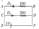
Two ideal diodes are connected to a battery as shown in the circuit. The current supplied by the battery is
1. 0.75 A
2. 0.5 A
3. 0.25 A
4. zero
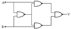
Truth table for system of four NAND gates as shown in figure is
1. 
2. 
3. 
4. 